RF PCB
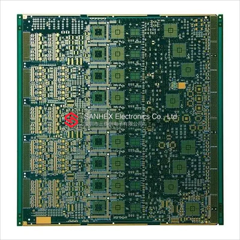
RF printed circuit board
- Industry:
- Communication
- Product:
- Communication Base Station
- Layer:
- 22
- Surface Treatment:
- ENIG
- Material:
- FR4
- Outer Layer Line Width/Spacing:
- 3mil
- Inner Layer Line Width/Spacing:
- 3.5mil
- Board Thickness:
- 2.45mm
- Minimum Hole Size:
- 0.1mm