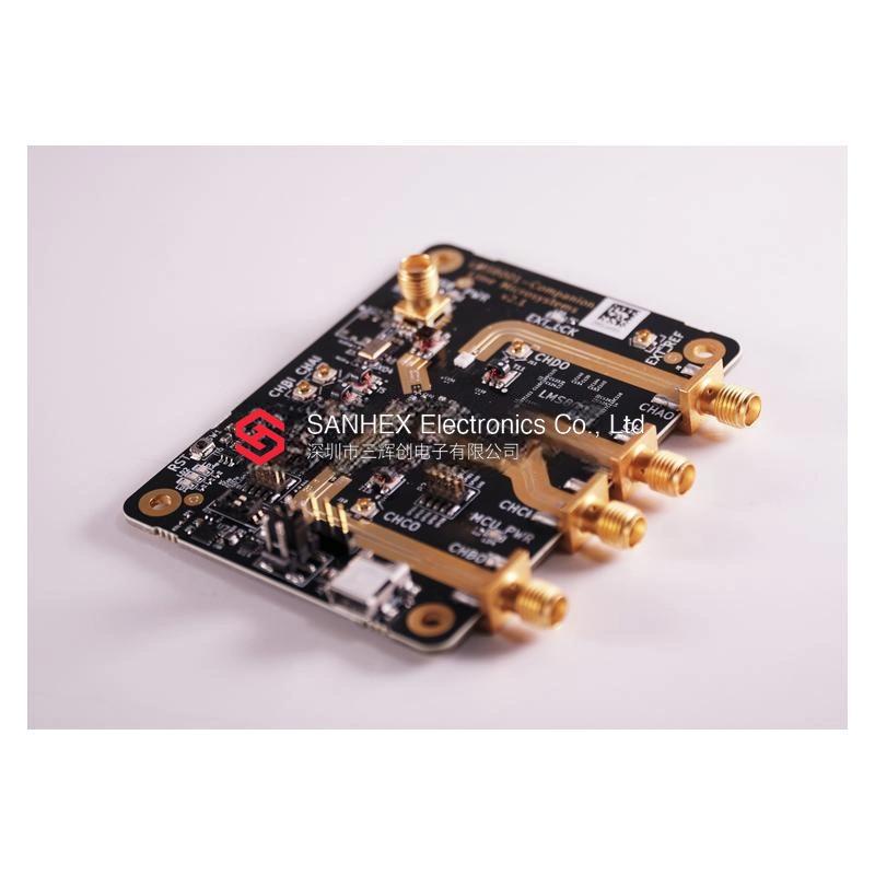
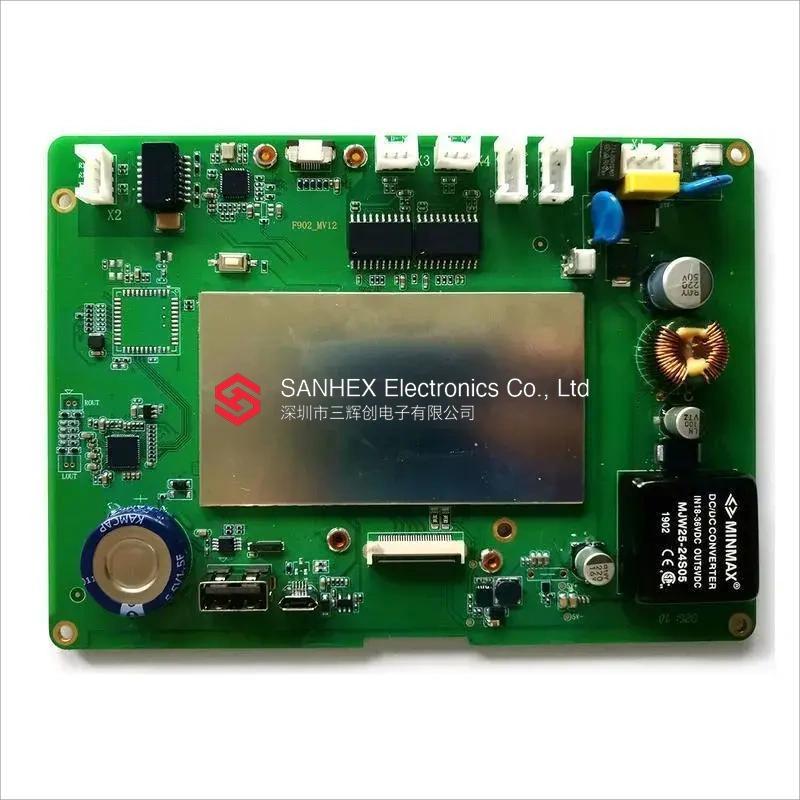
PCB Assembly
PCBA PROCESSING CAPABILITY
| Service types | Turnkey: PCB fabrication + component sourcing + SMT/DIP assembly + testing + packaging + shipping |
| Lead time | Prototype: ~15 working days Mass order: ~20–25 working days |
| Testing & inspection | AOI 100% for SMT; X-ray for BGA/QFN (as needed); Flying probe (FPT) / ICT / Functional test (optional) |
| Required files | Gerber files(CAM, PCB, PCBDOC); BOM list Assembly drawing (PDF); Test specification/program (if any) |
| PCB panel size | Single board minimum: 0.25 × 0.25 inches (6 × 6 mm) Panelized board minimum: 1.97 × 1.97 inches (50 × 50 mm) Maximum: 19.69 × 18.50 inches (500 × 470 mm) |
| Solder & processes | Lead-free halogen-free RoHS Water‑soluble or no‑clean solder paste Reflow / Wave / Selective soldering Conformal coating / Underfill (optional) |
| Assembly capabilities | 01005 passives BGA/VFBGA, QFN/CSP Double‑sided SMT assembly Fine pitch down to 0.3 mm (12 mil) BGA rework/reball THT/DIP hand soldering and rework |
| Accepted component packaging | Reel, Cut tape, Tube, Tray, Loose parts |
| Certifications & standards | ISO 9001 / ISO 13485 / IATF 16949 |
| Quantity & capacity | MOQ: 1; prototype / small / large‑volume supported |
| Optional value‑added services | Programming, burn‑in, conformal coating, potting, box build/assembly |