HDI PCB
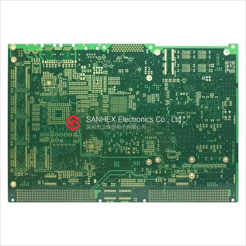
14-layer blind buried hole PCB circuit board
- Industry:
- Industrial Control
- Product Application:
- Equipment Motherboard
- Layer:
- 14
- Special Process:
- Blind Buried Hole
- Surface Treatment:
- ENIG
- Material:
- FR4
- Outer Layer Line Width/Spacing:
- 4/5mil
- Inner Layer Line Width/Spacing:
- 4/3.5mil
- Board Thickness:
- 1.6mm
- Minimum Aperture:
- 0.2mm