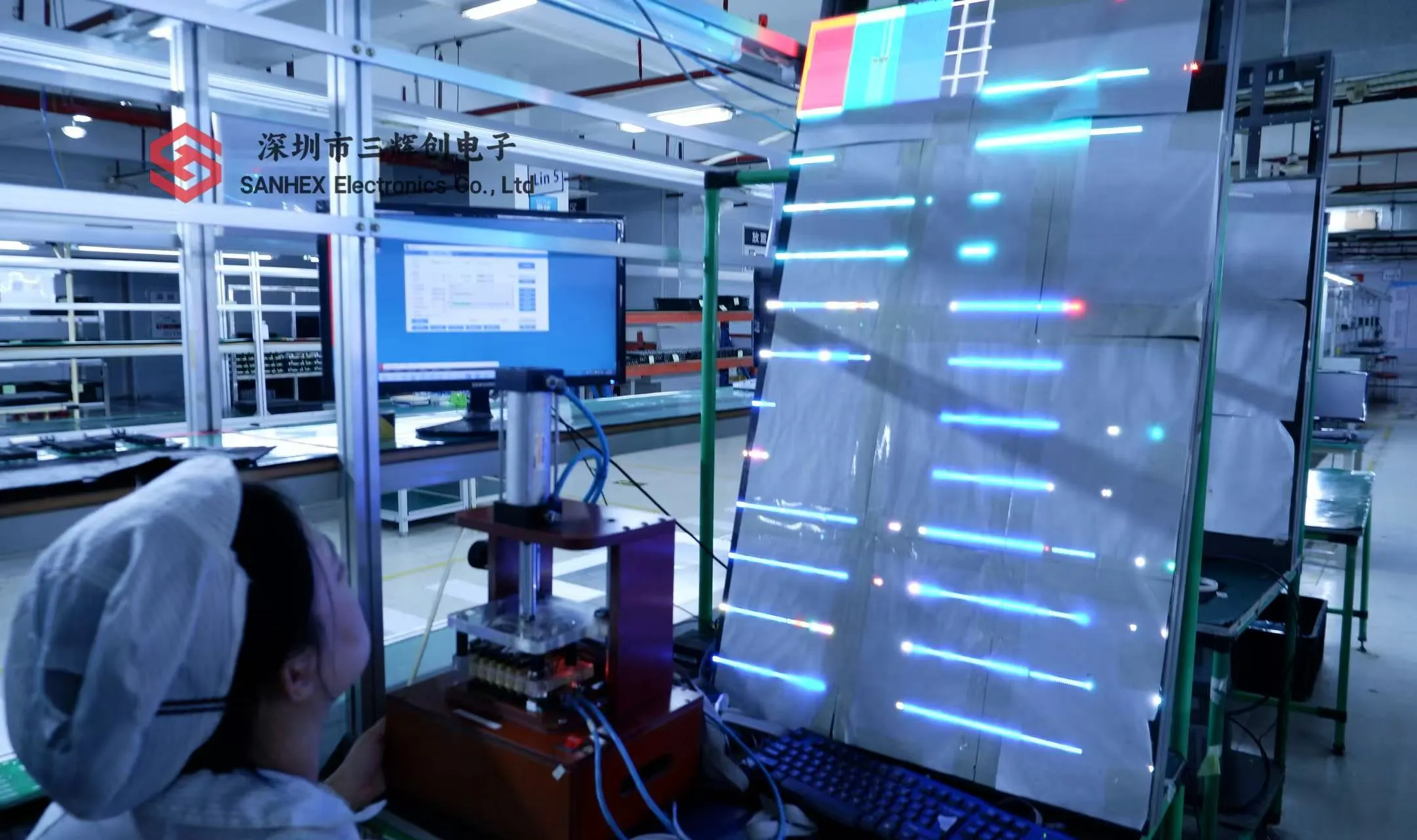
No single PCBA testing method can detect every manufacturing and functional defect. A practical test plan combines process inspection, electrical testing, and functional validation according to the board design, production volume, component package, and field reliability target.
For many assemblies, SPI and AOI provide fast process control, X-ray examines hidden solder joints, flying probe or ICT checks electrical connectivity and component-level faults, and FCT verifies whether the assembled board performs its intended function. The right combination is more important than the number of test methods listed on a quotation.
This guide explains what each method detects, where it fits in the assembly process, and how engineering teams can choose a cost-effective PCBA testing strategy.
PCBA Testing Methods at a Glance
| Test method | Primary purpose | Best suited for | Fixture required? | Main limitation |
|---|---|---|---|---|
| SPI | Measure solder paste before placement | All SMT production, especially fine-pitch work | No product-specific fixture | Cannot evaluate completed solder joints or electrical function |
| AOI | Inspect visible placement and solder conditions | Prototype through volume production | No | Cannot see hidden BGA/QFN joints or prove circuit function |
| X-ray | Inspect hidden solder joints and internal structures | BGA, QFN, LGA, bottom-terminated packages | Usually no dedicated electrical fixture | Does not verify firmware or full electrical behavior |
| Flying probe | Check nets and selected components without a bed-of-nails fixture | Prototypes and changing low-volume designs | No traditional fixture | Slower per board than fixture-based ICT |
| ICT | Test connectivity and component-level electrical conditions | Stable medium- and high-volume products | Yes, typically | Requires test access and fixture investment |
| FCT | Validate powered board behavior against requirements | Products where system operation must be verified | Usually a custom test setup | Quality depends on the completeness of the test specification |
These methods are complementary. Inspection identifies manufacturing process defects, electrical tests isolate assembly faults, and functional testing evaluates the board as an operating system.
1. Solder Paste Inspection (SPI)
SPI takes place immediately after solder paste printing and before component placement. A typical 3D SPI system measures paste height, area, volume, alignment, and shape on each inspected pad.
This early position in the process is important because insufficient paste, excessive paste, or stencil misalignment can later produce opens, bridges, tombstoning, and inconsistent joints. Correcting a printing problem before components are placed is usually more efficient than finding the same defect after reflow.
SPI is especially valuable for fine-pitch components, small passives, and boards with mixed pad geometries. However, it only evaluates the paste deposit. It cannot determine whether a component was placed correctly, whether the final joint is acceptable, or whether the circuit works.
For designs with narrow process windows, see our guide to 0.3mm fine-pitch assembly.
2. Automated Optical Inspection (AOI)
AOI uses cameras, controlled lighting, and image-processing rules to inspect visible features on an assembly. Depending on where it is installed, AOI can identify missing or shifted components, polarity errors, wrong visible markings, solder bridges, insufficient solder, lifted leads, and other surface-level defects.
AOI is effective as an inline quality gate because it is repeatable and provides process feedback. If the same defect appears across several boards, engineers can investigate placement data, stencil design, feeder setup, or reflow conditions before the issue affects a larger batch.
Its main limitation is line of sight. AOI cannot directly inspect solder balls beneath a BGA or other bottom-terminated package. It also cannot confirm that a correctly placed component has the right internal value or that firmware and interfaces operate correctly.
3. X-Ray Inspection
X-ray inspection is used when important solder joints are hidden from optical systems. It can reveal conditions beneath BGA, QFN, LGA, and similar packages, including bridges, opens, missing balls, solder distribution problems, and voiding patterns.
X-ray is commonly applied to first articles, high-risk package locations, process validation, and failure analysis. Whether every board or a defined sample is inspected should be based on package risk, customer requirements, production maturity, and the agreed control plan.
An X-ray image still requires correct interpretation. It provides structural evidence, not a complete electrical verdict. A joint may look acceptable while the board has a component-value, programming, or system-level fault. X-ray should therefore be combined with electrical or functional validation where those risks matter.
4. Flying Probe Test
Flying probe testing uses movable probes to contact test pads, component leads, vias, and other accessible points. It can check continuity, opens, shorts, and selected component measurements without manufacturing a traditional bed-of-nails fixture.
That flexibility makes flying probe attractive for prototypes, engineering validation builds, and low-volume products that may still change. Test programs can be updated more easily when a revision changes net access or component placement.
The trade-off is test time. Because probes move between test points, flying probe is generally slower per board than fixture-based ICT. Coverage also depends on physical access and the available design data. Dense boards with limited exposed test points may require boundary scan, functional test, or other complementary methods.
5. In-Circuit Test (ICT)
ICT uses electrical access to test individual nets and components on an assembled board. A fixture-based system can detect opens, shorts, incorrect or missing components, orientation issues, and out-of-range values where the circuit and access strategy allow.
The primary advantage is repeatable, fast testing for a stable production design. The primary cost is the fixture and test-program development. ICT is therefore usually more economical when the design is mature and the production volume justifies the initial engineering effort.
Test-point planning must begin during PCB design. Inadequate probe access, inaccessible ground references, or test points placed too close to tall components can reduce coverage or make the fixture unnecessarily complex. ICT provides component-level diagnostics but does not replace full functional validation.
6. Functional Circuit Test (FCT)
FCT powers the PCBA and verifies selected behavior against the product requirements. A functional test may check supply rails, current draw, digital and analog inputs, outputs, communication interfaces, sensors, relays, displays, firmware programming, or a controlled operating sequence.
FCT answers a different question from AOI or ICT: does the assembled board perform the functions defined by the customer? This makes it important for products where component-level inspection alone cannot demonstrate correct operation.
Functional testing is only as strong as its specification. A simple power-on check may miss interface, load, timing, or protection faults. A useful FCT plan defines test conditions, stimulus, expected response, tolerances, pass/fail limits, firmware version, and data-recording requirements. ICT and FCT are complementary rather than interchangeable because they verify different layers of the assembly.
How to Choose a PCBA Test Combination
The selection should follow the risks of the product rather than a fixed checklist.
Prototype and Engineering Builds
A common starting point is SPI, AOI, targeted X-ray for hidden joints, and flying probe where electrical access is available. FCT is added when the engineering team can define meaningful powered behavior. The objective is not only to reject bad boards but also to collect diagnostic information for the next design revision.
Low-Volume Production
Low-volume products often retain flying probe because design flexibility matters more than the cycle-time advantage of a dedicated ICT fixture. AOI remains useful for process control, while X-ray is applied according to package risk. A reusable FCT setup can provide strong value when the same functional requirements continue across batches.
Stable Medium- and High-Volume Production
When the design and forecast are stable, ICT may become more economical because its fixture cost is distributed across more units. SPI and AOI support inline process control, while FCT verifies product behavior. X-ray may be applied inline, to critical locations, or by sampling according to the agreed quality plan.
High-Reliability Applications
Medical, automotive, industrial, and other high-reliability products require a project-specific control plan. Testing may include tighter process controls, serial-number traceability, controlled firmware, recorded measurements, environmental screening, or customer-defined acceptance criteria. Industry labels alone do not determine the test stack; the actual product risk and contractual requirements do.
Design for Testability (DFT) Checklist
Testing becomes more effective and less expensive when access is designed into the board. During schematic and layout review, engineering teams should consider:
- Accessible test points for critical nets, power rails, and ground references
- Probe spacing and clearance from tall components or mechanical hardware
- Programming access for MCUs, memory, and programmable logic
- Isolation options for circuits that cannot be measured accurately in parallel
- Defined connector pinouts and safe power-up sequencing
- Diagnostic firmware or test modes for important interfaces
- Measurable pass/fail limits rather than subjective observations
- Board identification and serial-number strategy when traceability is required
DFT decisions should be reviewed before layout release. Adding reliable access after the board is built can require test compromises or a PCB revision.
What to Provide for a PCBA Test Quotation
Accurate testing quotations require more than Gerber files and a BOM. Provide the manufacturer with:
- Schematic, netlist, BOM, Gerbers, and Pick and Place data
- Required inspection and electrical test methods
- Firmware files, programming procedure, and checksum information
- Functional test steps with inputs, outputs, limits, and expected behavior
- Required cables, loads, mating connectors, power supplies, and communication tools
- Golden sample or known-good reference when available
- Data logging, serial number, and test-report requirements
- Expected prototype and production quantities
Defining these items early reduces quotation assumptions and prevents testing from becoming a late-stage delivery blocker. Our PCBA quotation file checklist explains the broader manufacturing data package, while our article on common PCBA project delays covers the schedule impact of late test definition.
PCBA Testing Standards and Acceptance Criteria
Testing requirements should reference the correct standards and customer specification. IPC-A-610J and J-STD-001J provide widely used assembly acceptance and soldering process criteria. They do not replace a product-specific electrical or functional test specification.
The purchase order, drawings, approved workmanship class, test procedure, and acceptance limits should agree before production starts.
Frequently Asked Questions
Which PCBA testing method is the best?
There is no universal best method. SPI and AOI control visible manufacturing processes, X-ray examines hidden joints, flying probe and ICT find electrical assembly faults, and FCT verifies intended behavior. The best plan combines methods that address the product's highest risks.
Can AOI replace X-ray inspection?
Not for hidden solder joints. AOI is effective for visible features, while X-ray is used for structures beneath BGA, QFN, LGA, and similar packages. Boards without hidden-joint risk may not need the same X-ray plan as a dense BGA assembly.
What is the difference between flying probe and ICT?
Flying probe avoids a traditional bed-of-nails fixture and is flexible for prototypes and changing designs, but it is slower per board. ICT uses dedicated access and is faster for stable production, but requires fixture and program investment.
Is functional testing always required?
It depends on the product and customer requirements. A visual or electrical inspection cannot prove that firmware, communications, sensors, or outputs work as intended. When those functions are important, an appropriately defined FCT is usually the direct validation method.
When should the test plan be defined?
Ideally during schematic and PCB layout development. Early planning allows test points, programming access, fixtures, firmware, and acceptance limits to be prepared before the first production build.
Conclusion
A reliable PCBA testing strategy is a sequence of risk controls, not a single final inspection. SPI controls solder paste, AOI checks visible assembly conditions, X-ray evaluates hidden joints, flying probe and ICT diagnose electrical faults, and FCT confirms defined product behavior.
SANHEX supports turnkey PCB assembly services from DFM and component sourcing through SMT/DIP assembly, inspection, programming, and project-specific testing. Test scope is reviewed against the design, production volume, package risk, and customer acceptance criteria.
Need a PCBA Testing Plan for Your Project?
Send our engineering team the following files for a testability review and PCBA quotation:
- Gerber files and Pick and Place data
- BOM and schematic
- Expected prototype and production quantities
- Firmware and programming instructions
- Existing test procedure, acceptance limits, or golden sample details
We will review the available test access, hidden-joint risks, production volume, and functional requirements before recommending a practical inspection and test combination.
Request a PCBA testing review: Email sales@sanhex.com or explore our turnkey PCB assembly services.