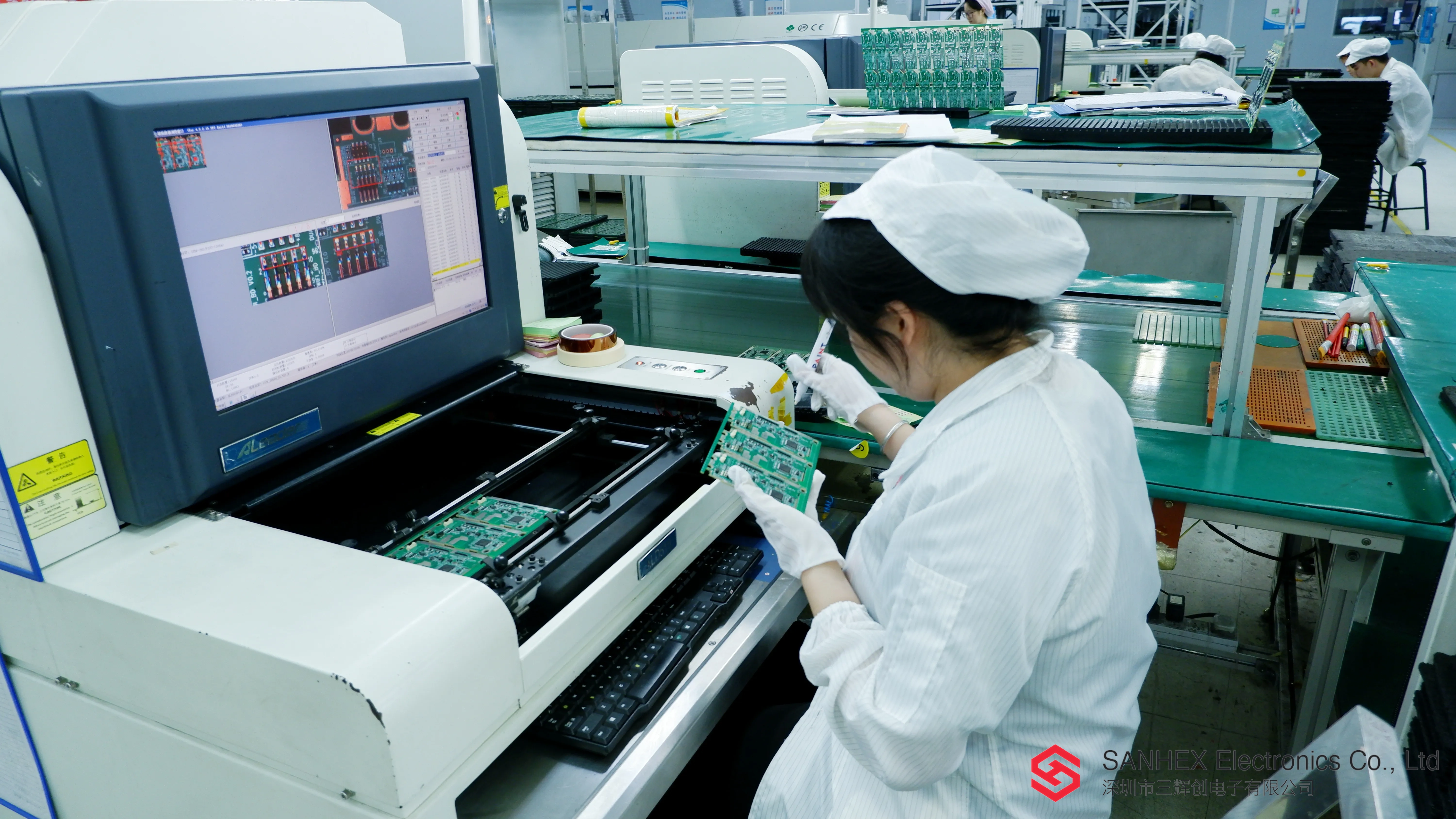
High-Density Interconnect (HDI) PCB technology represents a revolutionary advancement in printed circuit board design, enabling the creation of smaller, faster, and more reliable electronic devices. As consumer electronics demand increasingly compact form factors and higher performance, HDI PCBs have become essential for next-generation applications.
Understanding HDI PCB Technology
HDI (High-Density Interconnect) PCBs feature significantly higher wiring density per unit area compared to conventional PCBs. This is achieved through:
- Microvias: Laser-drilled holes with diameters typically 0.1mm or smaller
- Fine-pitch components: Components with pin pitches of 0.5mm or less
- Thin dielectric layers: Reduced layer thickness for improved signal integrity
- Advanced via structures: Stacked, staggered, and buried vias for complex routing
Key HDI Characteristics
Via Technology:
- Microvias: 0.1mm diameter or smaller, typically 0.05-0.08mm
- Via-in-Pad: Vias placed directly under component pads
- Stacked Vias: Multiple microvias stacked vertically
- Staggered Vias: Offset microvias for improved reliability
Layer Configuration:
- 1+N+1: Single microvia layer on each side
- 2+N+2: Two microvia layers on each side
- Any Layer: Microvias on any layer combination
HDI PCB Manufacturing Process
1. Design and Planning Phase
Design Rules:
- Minimum via diameter: 0.1mm (standard), 0.05mm (advanced)
- Minimum via pitch: 0.2mm
- Minimum trace width: 0.075mm
- Minimum spacing: 0.075mm
Layer Stackup Considerations:
- Core thickness: 0.1-0.2mm for microvia layers
- Dielectric constant: 3.4-4.5 for high-speed applications
- Copper thickness: 0.5-1.0oz for fine features
2. Manufacturing Process Steps
Core Preparation:
- Ultra-thin core materials (0.1-0.2mm)
- Precision copper foil application
- Surface treatment for microvia formation
Microvia Formation:
- Laser Drilling: UV laser for precise hole formation
- Plasma Etching: Alternative method for certain materials
- Desmear Process: Removal of resin smear
- Via Filling: Copper plating or conductive paste
Lamination Process:
- Sequential lamination for complex structures
- Controlled pressure and temperature
- Void-free bonding for reliability
Surface Finishing:
- ENIG (Electroless Nickel Immersion Gold)
- OSP (Organic Solderability Preservative)
- Immersion Silver for fine-pitch applications
HDI PCB Applications and Benefits
Primary Applications
Consumer Electronics:
- Smartphones: Mainboards with 8-12 layer HDI
- Tablets: High-density memory and processor integration
- Wearables: Ultra-compact sensor and communication modules
Computing Systems:
- Laptops: Motherboards with high-speed interfaces
- Servers: Multi-processor boards with advanced cooling
- Graphics Cards: High-performance GPU substrates
Medical Devices:
- Implantable Devices: Ultra-thin, biocompatible designs
- Diagnostic Equipment: High-precision sensor integration
- Portable Monitors: Compact, battery-powered systems
Automotive Electronics:
- ADAS Systems: Advanced driver assistance modules
- Infotainment: High-resolution display controllers
- ECU Modules: Engine and transmission control units
Technical Advantages
Size Reduction:
- 50-70% smaller footprint compared to conventional PCBs
- Higher component density per unit area
- Reduced weight for portable applications
Performance Benefits:
- Improved signal integrity with shorter trace lengths
- Reduced crosstalk through better layer planning
- Enhanced thermal management with optimized via placement
- Lower power consumption due to reduced parasitic effects
Reliability Improvements:
- Fewer solder joints with direct via-in-pad connections
- Improved thermal cycling performance
- Enhanced mechanical stability with optimized layer structure
Design Guidelines for HDI PCBs
1. Via Design Considerations
Microvia Specifications:
- Aspect Ratio: Maximum 1:1 for reliable plating
- Via Fill: Copper plating or conductive paste
- Via-in-Pad: Requires careful thermal management
- Stacked Vias: Limit to 2-3 levels for reliability
Via Placement Rules:
- Minimum 0.2mm spacing between microvias
- Avoid via-in-pad for large components
- Consider thermal expansion effects
- Plan for test point accessibility
2. Routing and Layout Guidelines
Signal Integrity:
- Differential Pair Routing: Maintain consistent spacing
- Impedance Control: 50Ω single-ended, 100Ω differential
- Length Matching: ±0.1mm for critical signals
- Via Stitching: Ground vias for EMI reduction
Power Distribution:
- Power Plane Design: Dedicated layers for power and ground
- Decoupling Capacitors: Strategic placement near ICs
- Via Current Capacity: Consider current density limits
- Thermal Management: Heat spreading and dissipation
3. Component Placement Strategy
Fine-Pitch Components:
- BGA Packages: 0.5mm pitch or smaller
- QFN/QFP: Lead-free soldering considerations
- Passive Components: 0201 or 01005 packages
- Connectors: High-density, board-to-board types
Thermal Considerations:
- Heat Sink Integration: Thermal vias and pads
- Component Spacing: Adequate clearance for cooling
- Thermal Relief: Via design for thermal management
- Material Selection: High thermal conductivity substrates
Manufacturing Challenges and Solutions
Common HDI Manufacturing Issues
Via Formation Challenges:
- Laser Drilling: Precise control of hole size and shape
- Via Filling: Complete copper plating without voids
- Desmear Process: Complete resin removal
- Plating Uniformity: Consistent copper thickness
Lamination Difficulties:
- Void Prevention: Controlled pressure and temperature
- Layer Alignment: Precise registration for microvias
- Material Compatibility: Matching thermal expansion
- Bond Strength: Adequate adhesion between layers
Quality Control:
- X-ray Inspection: Via fill verification
- Cross-section Analysis: Via quality assessment
- Electrical Testing: Continuity and isolation
- Thermal Cycling: Reliability validation
Advanced Manufacturing Techniques
Sequential Lamination:
- Build-up Process: Layer-by-layer construction
- Via Formation: Laser drilling after each lamination
- Plating Process: Copper deposition in microvias
- Surface Preparation: Cleaning and activation
Advanced Materials:
- Low-Loss Dielectrics: Reduced signal attenuation
- High-Tg Materials: Improved thermal performance
- Flexible Substrates: Bendable HDI applications
- Metal Core: Enhanced thermal management
Cost Considerations and Optimization
HDI PCB Cost Factors
Manufacturing Complexity:
- Layer Count: Additional layers increase cost
- Via Density: Higher via count requires more processing
- Material Selection: Premium materials for performance
- Testing Requirements: Comprehensive quality assurance
Design Optimization:
- Via Minimization: Reduce unnecessary vias
- Layer Reduction: Optimize layer count
- Standard Materials: Use proven, cost-effective substrates
- Panel Utilization: Maximize board area efficiency
Cost-Benefit Analysis
Initial Investment:
- Design Tools: Advanced CAD software
- Prototyping: Higher initial development cost
- Testing: Comprehensive validation requirements
- Tooling: Specialized manufacturing equipment
Long-term Benefits:
- Size Reduction: Smaller enclosures and materials
- Performance: Improved functionality and reliability
- Market Position: Competitive advantage in compact designs
- Scalability: Easier integration in complex systems
Future Trends in HDI Technology
Emerging Applications
5G and Beyond:
- Millimeter Wave: High-frequency PCB requirements
- Massive MIMO: Antenna array integration
- Edge Computing: Compact processing modules
- IoT Devices: Ultra-low-power, small-form-factor designs
Artificial Intelligence:
- Neural Processing: High-density computing boards
- Machine Learning: Accelerator card integration
- Edge AI: Local processing capabilities
- Quantum Computing: Cryogenic PCB requirements
Technology Evolution
Advanced Materials:
- Low-Dk Dielectrics: Reduced signal loss
- High-Tg Substrates: Improved thermal performance
- Flexible HDI: Bendable and foldable applications
- Biocompatible: Medical and wearable applications
Manufacturing Innovations:
- 3D Printing: Additive manufacturing for complex structures
- Nano-materials: Enhanced electrical properties
- Automated Assembly: Robotic component placement
- AI-Driven Design: Machine learning optimization
Best Practices for HDI PCB Design
Design Phase Recommendations
Planning and Analysis:
- Signal Integrity Simulation: Pre-layout analysis
- Thermal Modeling: Heat dissipation planning
- Manufacturing Review: DFM considerations
- Cost Optimization: Balance performance and cost
Collaboration:
- Early Engagement: Involve manufacturer early
- Design Reviews: Regular milestone assessments
- Prototype Testing: Validation before production
- Continuous Improvement: Iterative optimization
Manufacturing Partnership
Vendor Selection:
- HDI Experience: Proven track record
- Quality Certifications: ISO 9001, IPC standards
- Technical Support: Design assistance capabilities
- Supply Chain: Reliable material sourcing
Communication:
- Design Guidelines: Clear specifications
- Regular Updates: Progress monitoring
- Issue Resolution: Quick problem solving
- Knowledge Transfer: Technology sharing
Conclusion
HDI PCB technology represents the future of electronic design, enabling the creation of smaller, faster, and more reliable devices. As applications continue to demand higher performance in smaller packages, HDI PCBs provide the technical foundation for next-generation electronics.
Key Takeaways:
- HDI PCBs enable 50-70% size reduction while maintaining or improving performance
- Microvia technology is the cornerstone of HDI design
- Manufacturing complexity requires specialized expertise and equipment
- Cost optimization balances performance requirements with manufacturing feasibility
- Future applications will continue to drive HDI technology evolution
At SANHEX Electronics (深圳市三辉创电子有限公司), we specialize in HDI PCB design and manufacturing, providing comprehensive solutions from concept to production. Our experienced engineering team and state-of-the-art manufacturing capabilities ensure your HDI projects meet the highest quality standards.
Ready to start your HDI project? Contact our technical team today for a detailed consultation and quote. Visit sanhex.com or reach out to us at sales@sanhex.com to discuss your specific requirements.
This comprehensive guide provides the foundation for understanding and implementing HDI PCB technology. The choice of HDI design approach depends on your specific application requirements, performance targets, and cost constraints. SANHEX Electronics (深圳市三辉创电子有限公司) is here to help you navigate these decisions and implement the most effective HDI solution for your success.